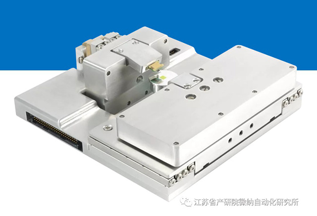
SEM compatible with atomic force microscope: em-afm
EM-AFM
Em-afm nano operating system provides the ability of atomic force microscope imaging and quantitative measurement of nano force in SEM electric mirror. It makes the best combination of SEM and AFM, and provides high-speed and high-resolution 3D morphology imaging and real-time observation of nano force interaction at micro nano and sub nano scales.
Product characteristics
| Synchronous AFM and SEM imaging |
Quantitative measurement of nano force by nano indentation |
| Fully compatible with the mainstream SEM on the market |
Vacuum load lock compatible |
| Ultra high resolution topography scanning |
High operation stability, free from SEM electron beam interference |
Application case
Sem-afm image fusion
SEM imaging has the advantages of high lateral resolution and scanning rate. Combined with the three-dimensional morphology information provided by AFM imaging, new and comprehensive information can be obtained.
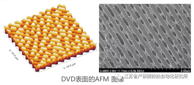
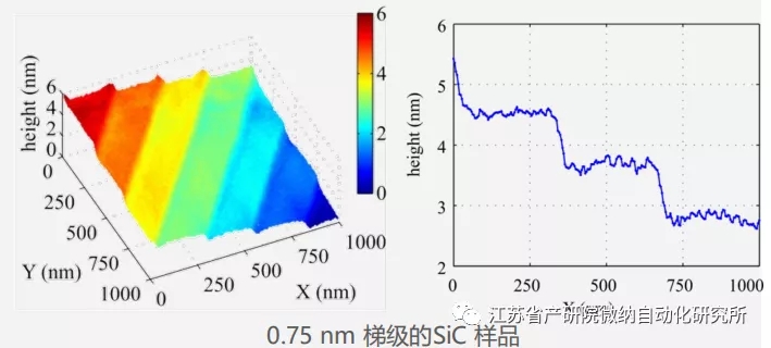
Sub nano imaging resolution
The full closed-loop coding system ensures that ultra-high morphological imaging resolution and sub nano imaging resolution can be obtained without image distortion.
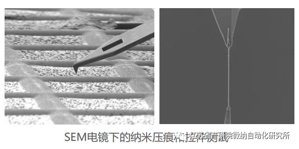
Nanoindentation and tensile testing
The nanomechanical properties of the samples can be measured by nano indentation and nano tensile test techniques in the instrument. The indentation and tensile process can be observed in real time under SEM. The special software provides built-in calculation tools for analyzing and displaying the obtained measurement data.
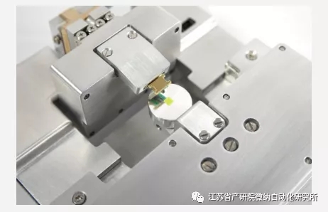
High vacuum environment / SEM compatible
The compact AFM is compatible with most SEM and fibs on the market and can be installed and disassembled in seconds. The system allows a small working range (5mm) and is compatible with standard SEM analysis techniques (such as EDS, EBSD, WSD).
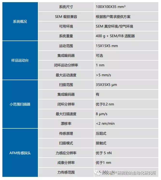
Specification parameters